12 laboratories
Clean rooms are the mandatory working environment in all industrial sectors and research laboratories that require strict control in terms of cleanliness and control of the working environment. This is particularly the case in the field of microelectronics, nanotechnologies and nanosciences. Today, the lateral dimension of commonly produced components is sub-micrometric (100 nm), and can reach the nanometric/molecular scale for the best platforms and laboratories. In order to achieve these accuracies on a regular basis and to guarantee the quality and reproducibility of the processes, it is essential to be free from any source of uncontrolled contamination (dust) and to work at constant temperature and hygrometry.
The construction and operation of a clean room represents a very heavy investment. The cost of installing the empty clean room alone can be more than €10,000/m2, to which must be added all the equipment. This is why these investments are often pooled, for example, by a consortium of companies that wish to develop a common technology. In terms of training and research, France is particularly well equipped with several networks of specific and complementary platforms, capable of meeting the various needs expressed for the implementation of applied or very basic research and development projects. Renatech is the French academic network of state-of-the-art equipment in the field of micro and nanotechnology led by the CNRS, open to the entire academic community and to industry. Second circle technology centres or proximity centres with very specific technological fields complete the Renatech network and allow the development/creation of new technological fields.
Within this coherent network, CEMES-CNRS has a unique infrastructure in the Picolab building with equipment adapted to classic nano-fabrication processes and a totally original ultra-high vacuum process including atom-by-atom fabrication processes.
The CEMES clean room is open to the scientific community: for academic researchers within or outside CEMES but also for private companies. The service aims to provide expertise, tools and instruments dedicated to micro- and nanofabrication for fundamental and applied research, education and training.
The department manages the entire 450m2 clean room, which is segmented into several dedicated rooms, classified as ISO Class 4 to 7. The ISO Class 4 room is dedicated to current lithography processes and the development of advanced atomic technologies.
Experimental techniques:
Human skills:
Optical and electron beam lithography
Two sputtering machines, annealing furnaces
The “Ultimate Microscopies” branch of the CP-UHV department of CEMES is equipped with 3 experimental equipments operating under ultra-high vacuum (UHV), installed in the low noise clean rooms of the PicoLab building :
1. LT-STM/Qplus (Low Temperature STM): the low temperature STM
Low-temperature scanning tunnelling microscope (STM) that can work at a temperature of 5K in STM mode and/or in non-contact AFM mode (NC-AFM). Equipped to prepare crystalline surfaces under UHV and to deposit thin insulating layers, it allows the deposition of metals or molecules at low temperature.
2. The DUF (DiNaMo UHV Factory): the factory under UHV
Designed and developed at CEMES, this equipment offers a complete device for measuring the electronic properties of a single molecule in planar configuration on an insulating surface. It is composed of 5 UHV chambers connected by a transfer tube under UHV: i) molecular beam epitaxy (MBE) frame, ii) preparation chamber for tips and molecule deposition, iii) low energy and controlled ion source, iv) high sensitivity NC-AFM/KPFM microscope and v) STM+NC-AFM/KPFM microscope equipped with the nanostencil technique.
3. The LT-UHV 4-STM/Qplus + SEM: the “4 spikes”
Low temperature microscope (4K) with 4 independent STM heads and a FEG-SEM column. One of the STM heads is also equipped with the Qplus module for NC-AFM measurements at 5 K. The unit is connected to a preparation chamber under UHV (possibility of multiple sublimations of molecules) and to another chamber equipped with a UHV transfer printer.
About ten permanent and non-permanent CEMES researchers are developing their research on this equipment.
This microscope was the arena in which the 1st edition of the NanoCar Race, a race of molecules on a 100 nm track, took place in April 2017. The 2nd edition of this scientific competition took place in March 2022.
The “Local Probe Microscopy” branch of the CP-UVH service brings together a set of near-field surface imaging techniques in air. It is divided into a service activity and a research activity.
1) The service activity is based on two Bruker commercial microscopes, one of which is integrated in a clean room and is equipped with a nano-positioning table. The service offers access to measurements of:
– Topography (AFM contact or tapping mode, STM) in air or liquid
– Imaging of lateral friction forces (LFM)
– Magnetic Force Imaging (MFM)
– Electrical Force Imaging (EFM)
– Surface Potential Imaging (KFM)
– Piezoelectric Force Imaging (PFM)
– Force curves
Near-field microscopy, or local probe microscopy, allows 3-dimensional observations, on scales from 1 nm to 100 µm, on all types of samples: surfaces (metallic, semiconducting or insulating), nano-objects (nanoparticles, nano-structures), molecules, biological samples…
The department is also equipped with a Bruker Dektak 150 contact profilometer. Located in a clean room as close as possible to the nanofabrication processes, this device is ideal for rapidly measuring the profile of a surface in order to determine its roughness or geometry on a micro or nanometric scale.
Methods of carrying out the measurements:
– Services by the person in charge, with or without the presence of the applicant
– Training of the applicant in order to be autonomous on the microscope (to be considered for large measurement campaigns)
Physical constraints on the samples for the microscope outside the clean room:
– The geometrical configuration of the equipment requires calibration of the sample format: the useful area to be observed must be located in the centre of the sample, in an area of approximately 5×5 mm², with the total dimensions of the sample not exceeding 1 cm (W) x 1 cm (L) x 0.8 cm (D)
– The sample may be very small or of any shape
How to access:
– Contact the person in charge of the activity (contact details below)
– For applicants already trained, bookings on GRR via the CEMES intranet site
Conditions of access:
– The service is open in priority to members of the laboratory
– The service is also open to external parties, institutions or companies
Pricing: at full cost, unit of work (UO): half a day
– Academic clients: 30.35€ to 99.53€ per UO, depending on the source of funding
– Other clients: 727.77€ per UO
For more information, please contact Grégory Seine, 05 62 25 79 64
2) The research activity also relies on a commercial Bruker microscope, but transformed to operate in the near-field optical mode “PSTM” (Photon Scanning Tunneling Microscope) and in the STM stimulated photon emission mode “LE-STM”. Although research-oriented, this microscope can be used with all the usual AFM modes. It allows to associate the 3D topography of AFM or STM with a mapping of the photonic emission in near field obtained by optical excitation of the sample (photoluminescence type) or electronic (cathodoluminescence type).
The microscope has a laser line (violet to near infrared range 457 nm – 1000 nm) allowing the samples to be excited in total reflection through a prism. Photon collection is via a thinned optical fibre (in PSTM mode) or not (in LE-STM mode). The collected light can be routed to a photomultiplier (photon counting) or a spectrometer (spectral analysis).
Responsable : Renaud Péchou, 05 62 25 78 95
One ion implanter with low energy module.
(Grégory SEINE (Resp.), Frédéric NEUMAYER)
Ion implantation involves introducing ions into a material to modify its properties. For example, in microelectronics, the ion implanter is used to boost semiconductor materials.
At CEMES, ion implantation is one of the physical ways of synthesising nanoparticles.
The CEMES ion implanter is a VARIAN 200-2A (200 keV) model, with a specific feature: an “Ultra Low Energy” (ULE) module allowing implantation at energies from 0.6 keV. It was renovated in early 2016.

Grégory SEINE (Resp.), Frédéric NEUMAYER
Thanks to the ULE module, this equipment makes it possible to manufacture nanocrystals (after annealing in one of the furnaces of the Growth Link Department) by controlling:
The ion species that can be implanted are the following: Si, Ag, Au, N, Ar, H and He. In connection with the activities of the laboratory, the implantations carried out at CEMES concern applications in plasmonics and photovoltaics, microelectronics (transistors) or the implementation of the Smart Cut™ process.

The ATP platform thus provides researchers with a framework to accompany them from A to Z in the conduct of a nano-fabrication process, from development to characterisation: assistance in the choice of techniques, training in the use of instruments, assistance in the analysis of results and, more generally, management of the various phases of the process.
To take a virtual tour of the clean room and its equipment, click here!
Chips on inorganic support
“Sustainable development” organic chips
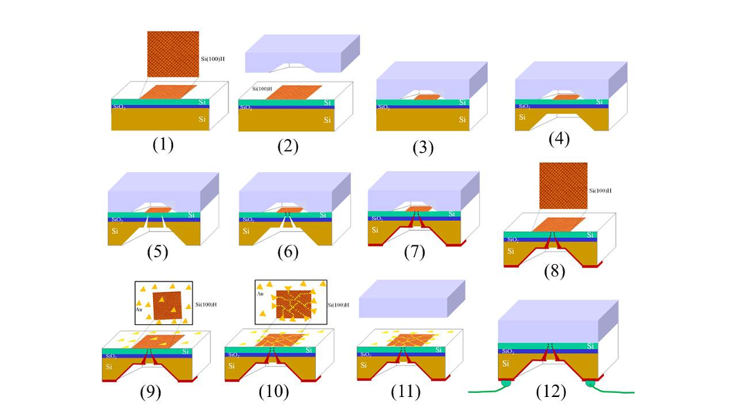
This “peer-to-peer” process with a UHV suitcase for transfer between stations concerns the development of 1st generation Atom Tech chips (2012 – 2025) – As started in C. Joachim’s “Atom Tech” group at IMRE, A*Star (Singapore) and with the European AtMol Project.
« Advances in Atom and single Molecule-Machines » Vol. 7, Fig. 2, p. 113 (2015)
Station 1: Front side preparation of the substrate by Molecular Beam Epitaxy (MBE) and STM imaging (Appl. Surf. Sci., 288, 83 (2014), AIP Adv. 5, 067108 (2015), Phys. Rev. B, 97, 081302(R) (2018))
 MBE in DUF
  LT-UHV STM/Qplus
Station 2: Manufacture of the front cover by Reactive Ion Etching (RIE)
 RIE
RIE
Station 3: Encapsulation in UHV
(N° WO 2009/022982 19 February 2009, Int. Patent classification: H01L 21/768 (2006.01) B82B 3/00 (2006.01), US patent: US2011/0018138A1)
Station 4: Backside engraving by RIE to free the front-rear passage by the “Via” technique
J. Vac. Sci. Tech. B, 28, 978 (2010)
Stations 5 to 7: Backside contacts by Focused Ion Beam (FIB) and decomposition of organo-metals
J. Vac. Sci. Tech. B, 28, 978 (2010)
 FIR
FIR
Station 8: Verification of the surface by LT-UHV-STM imaging and localisation of the emergence of the “Via”.
 LT-UHV STM/Qplus
Station 9: Metal contact nano-pads by UHV deposition
J. Vac. Sci. Tech. B., 28, 484 (2010)
 DUS
DUS
Station 10: Construction and testing (front side) of the atomic or molecular circuit by LT-UHV-4-STM Appl. Surf. Sci., 288, 83 (2014)
 LT-UHV 4-STM
Station 11: UHV encapsulation in the LT-UHV 4-STM printing chamber
Station 12: Final electrical test outside UHV
J. Vac. Sci. Tech. B, 28, 978 (2010)

The technological challenge is to switch the entire process to our integrated DUF (Dynamo UHV Factory) micro clean room in order to achieve the 2nd generation of Atome Tech chips, with the entire process taking place under UHV.

Progressive transition of each station and stage of nano-fabrication to renewable processes and materials (Techno-cyclable with their biocompatibility key).
“Give me the genes of a computer and I will program you a bacterium to bio-fabricate it and another bacterium to bio-decompose it molecule by molecule”
Inspired by:
K. Ulmer
Proceeding of the Molecular electronic Device Workshop
March 1981, Washington DC 23-24
Library of Congress ref. 12484,
Naval Research Lab ref. MR 4462
Les Bio-Transistors, La microélectronique du XXI siècle
J. De Rosnay,
La Recherche, 12, 870 (1981)
« Computers and the Environment »
R. Kuehr & E. Williams (Eds)
Kluwer Academic Publishers (2003)
« Nanosciences : la révolution invisible » p. 13
C. Joachim & L. Plévert
Editions du Seuil (2008)
« Radical Abundance »
K.E. Drexler
Published by PublicAffairs (Perseus Books Groups) (2013)