High refractive index dielectric nanostructures (typically silicon nanostructures) exhibit original optical properties related to the presence of optical resonances (Mie resonances) depending on their shape and dimensions. They are more and more studied as alternatives to plasmonic nanostructures to exalt and control the light-matter interaction at the sub-wavelength scale. The applications, concern photovoltaic devices, colored pixels, meta-surfaces, nonlinear optics and quantum light sources.
In figure 1, complex shaped nanostructures optimized by a reverse design approach (evolutionary multi-objective optimization algorithm, coupled with numerical simulations) show light scattering properties tunable according to the wavelength and polarization of the light.
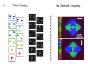
Figure 1: Si nanostructures modeled by evolutionary algorithm to optimize light scattering efficiency at two wavelengths and two polarizations. Left: pixel design (simulations and scanning electron microscopy images of structures produced by electron lithography). Right: polarization-filtered dark-field optical microscopy images of pictograms fabricated from the pixels obtained by inverted design
The high index dielectric nanostructures behave as nano-antennas capable of transforming a light wave propagating in space into a wave localized in and around the nano-antenna. This property allows to modify the emission of light by emitters placed in the near field of the nanostructure (Purcell effect). In figure 2, the light emission of a rare earth ion (Eu3+) doped thin film deposited on a Si nanostructure is strongly modified by the presence of the nanostructure. Moreover, the photoluminescence map corresponding to the magnetic dipolar emission at 590 nm is very different from that of the electrical dipolar emission at 610 nm. This remarkable property is due to the modification of the electric and magnetic photon densities of states around the nanostructure.
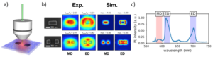
Figure 2: (a) laser beam scanning of Eu3+ doped thin film for photoluminescence (PL) mapping; (b) comparison of the maps (exp.) of the electric and magnetic dipole transitions with the electric and magnetic photon densities of states (sim.); (c) PL spectrum showing the magnetic (590 nm) and electric (610 nm) dipole transitions.
The presence of resonances also allows to modify or improve non linear properties such as the generation of second harmonic (SHG). Thus, in the absence of resonance no SHG is detected while a relatively intense emission is observed if the resonances coincide with the fundamental and/or the harmonic (figure 3).
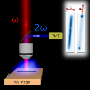
Figure 3: experimental setup for nonlinear optics and second harmonic maps (2ω) for two polarizations of the excitation (ω)
The different resonances as a function of silicon nanowire diameter also provide access to different SHG contributions. In Figure 4, two wires of different sizes excited in the same way emit SH of different origins. In the first case (small diameter wire), the SH is due to strong electric field gradients in the bulk and in the second, to a contribution from the surfaces.
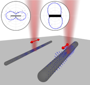
Figure 4: Rotation of the second harmonic polarization as a function of the diameter of silicon nanowires excited by radiation polarized along the wire axis
Funding: ANR HiLight (2020-24), EUR NanoX 2DLight (2019-2021)
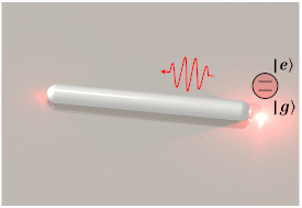
Quantum Plasmonics & Nano-Optics aims at transposing to 2D certain concepts of quantum optics by replacing the usual cavity mode by a plasmon mode supported by a metal nanostructure or by a photonic mode in a dielectric structure with an appropriate geometry. Surface plasmons are longitudinal modes that exist at the interface between a metal and a dielectric and allow for two-dimensional (2D) signal propagation along with confinement and field enhancement in subwavelength volumes. On the other hand, dielectric nanostructures support photonic modes with similar confinement, exaltation and propagation properties. The quantum regime requires the generation of single elementary excitations and this can be achieved by coupling one or more single photon emitters [1] to plasmonic or photonic cavities. This field of single excitations can lead to fascinating regimes where photon unbundling, quantum interference and entanglement could be observed in metallic or dielectric structures. In the context of quantum technologies, this allows to consider the development of elementary bricks based on the quantum properties of light for information transfer and control.
Contact: Aurélien Cuche

Figure 1: Left – Confocal photoluminescence map of single nanodiamonds containing NV- colored centers. Right – Photoluminescence spectrum of the negatively charged NV center (The photon unbundling curve inserted is from reference [1]) ©CEMES-CNRS

Figure 2: Left – Illustration of a nanodiamond containing a single NV center exciting plasmons propagating in a hexagonal plasmonic cavity. Center – Experimental luminescence spectrum of a single NV center coupled to such a hexagonal cavity in crystalline gold (inset autocorrelation curve). Right – Wide field images of the luminescence of the same nanodiamond coupled to this 2D crystalline plasmonic cavity (8 µm from the left end to the right end). It is possible to see the propagation of the 2D signal through the plasmons. The results are from reference [2] (This work is a collaboration between the NeO and GNS groups of CEMES and ETH Zurich). ©CEMES-CNRS

Figure 3: (a) Scanning electron microscopy image of the gold colloidal cavity (8 µm from the left end to the right end) after focused ion beam (FIB) shaping. (b) Wide field images of the luminescence of the nanodiamond coupled to the same crystalline 2D plasmonic cavity after FIB shaping via the addition of a hole array. (c) Simulation of the described system. (This work is a collaboration between the NeO and GNS groups of CEMES and ETH Zurich). ©CEMES-CNRS
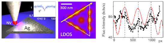
Figure 4: Left – Schematic representation of a scalar & quantum emitter attached to the apex of a NSOM tip [3] and scanned over a 2D silver nano-cavity.
Center – Simulation of the optical local density of states (LDOS) above a 900 nm square cavity. Right – Comparison of LDOS and fluorescence signal along a line above the structure shown by the yellow arrow in the center image. The results are from reference [4] (This work is a collaboration between Institut Néel, ICB laboratory and the NeO and GNS groups of CEMES). ©CEMES-CNRS
Figure 5: Top – Wide field images of the luminescence of a nanodiamond containing three NV centers coupled to the end of a 7 µm long silicon nanowire. The electron microscopy image of this nanosized wire is shown as an insert. Bottom – Autocorrelation curves measured directly on the nanodiamond (in) and after photon propagation in the nanowire (out). These curves show the same photon ungrouping showing the quantum nature of the light source. The results are from reference [5] (This work is a collaboration between LAAS, ICB laboratory and the NeO group of CEMES). ©CEMES-CNRS

Figure 6: Left – Two different magnification atomic force microscopy (AFM) images of nanodiamonds positioned in a controlled way by AFM nanoxerography on an SOI substrate. Center – Confocal photoluminescence image of the nanodiamond presented in AFM in the left image. Right – Autocorrelation curve showing photon unbundling acquired on the same nanodiamond. (This work is a collaboration between the NeO group of CEMES, the Nanotech group of LPCNO and LAAS). © CEMES-CNRS

Figure 7: Left – Optical dark field scattering images of silicon nanostructures (dimers) lithographed on an SOI substrate. Center – Electron microscopy image of the dimer surrounded by an orange circle on the left image (top). Confocal photoluminescence image of a nanodiamond positioned by AFM nanoxerography in the center of the dimer shown above (bottom). Right – Autocorrelation curve showing photon unbundling acquired on the same nanodiamond. (This work is a collaboration between the NeO group of CEMES, the Nanotech group of LPCNO and LAAS). ©CEMES-CNRS
[1] Y. Sonnefraud et al., Opt. Lett. 33, 611 (2008).
[2] U. Kumar et al., Nanoscale 12, 13414 (2020).
[3] A. Cuche et al., Nanolett. 10, 4566 (2010).
[4] A. Cuche et al., Phys. Rev. B 95, 121402(R) (2017).
[5] M. Humbert et al., Phys. Rev. Applied 17, 014008 (2022).
[6] M. Humbert et al., Nanotechnology 33, 215301 (2022).
[7] M. Humbert et al., in pparation (2022).

In the framework of our research in the fields of nano-optics and nano-photonics, we have developed new concepts, adapted theories as well as flexible and reliable numerical codes in order to describe the complex architectures associated with our current experimental measurements. Among the different theoretical objectives related to our activity, we can mention the general theory of Dyadic Green’s functions for electromagnetic calculations (field mapping, photonic and plasmonic LDOS, heat dissipation and temperature rise, far-field and EELS spectra) as well as numerical tools to describe plasmon-molecule interactions in the near-field (de-excitation rates, emission signals from a molecule, Maxwell-Bloch equations).
Contact: Christian Girard
The study of the fundamental aspects and the optimization of the functionalities of complex nano-optical systems, self-assembled on surface, or shaped by electron lithography (colloidal plasmonic superstructures, hybrid dielectric-plasmonic components, …) requires an important support for both theoretical modeling and numerical simulations. For example, understanding how surface plasmons couple to nearby quantum emitters (molecules, NV centers in diamond, quantum dots, …) is one of the major questions associated with our current experimental developments. Among the theoretical challenges related to these experimental studies, we can mention (i) the study of the properties of the emission signals and the statistics of the emitted photons of a quantum system coupled to a complex nano-optical structure, including metallic or hybrid materials, (ii) and (iii) the development of specific numerical tools implemented on an intensive parallel computing machine (EOS), allowing for example to simulate the two-photon luminescence (TPL) and the local plasmonic density of states (SP-LDOS), (iv) the study of the manipulation on surface via optical and electrical forces, and (v) the precise evaluation of the dissipation in plasmonic structures.
These different topics are currently studied thanks to a set of FORTRAN codes developed in-house, which are all dedicated to the study of sub-wavelength optical properties of complex systems. To date, these dedicated programs have been developed and improved within the NeO group. They are generally based on the general theory of 3D dyadic Green’s functions (GDF). When necessary, these tools are complemented by other theoretical tools for the description of phenomena such as optical and electrical forces, or van der Waals energy.
More recently, pyGDM has been developed at CEMES. It is a python toolbox (open source) for the realization of electro-dynamic simulations in nano-optics. pyGDM is also based on the Dyadic Green function (GDM) method.
Recently, we have developed a concise theoretical framework that can reproduce and analyze photon emission statistics as experimentally acquired from hybrid architectures composed of a quantum emitter coupled to a complex metallic or dielectric nanostructure. By solving directly the optical Bloch equations, all illumination regimes are accessible within the same theoretical framework. The obtained equations provide information on the mechanisms responsible for the modification of photon unbundling (spatial or polarization control, plasmon resonance effect, …). Our method allows direct comparison with current experimental work on simple structures (see Fig. 1), but can be generalized to treat more complex systems positioned at the surface of a sample. This formalism is currently applied to the study of energy transfer and coupling efficiency between plasmonic structures and two-level quantum systems.

Figure 1: Example of a photon unbundling signal calculated in the vicinity of a single gold particle [1].
[1] Marty el al, Phys. Rev. B 82, 081403,R (2010).
For metallic objects, the excitation wavelength is an important parameter. Excitation of surface plasmons causes a characteristic exaltation of the field that increases the intensity of the incident electromagnetic wave. Different physical quantities can be used to characterize the spectroscopic properties of self-assembled plasmonic systems: the near-field optical spectra which will give the variation of the near-field optical intensity at a given location R above the sample as a function of the incident wavelength, and the far-field extinction spectrum. Both quantities can be deduced from the optical electric field induced in the metal. For example, in the dyadic Green’s function (GDF) method, the local field distribution induced by external illumination is expanded onto a 3D mesh constructed within the particle volume. This has been used to simulate near-field optical spectra and images in close proximity to complex colloid assemblies.

Figure 2: Example of GDF simulation near a set of gold cubes deposited on a glass surface: Left: top view of the structure. Right: optical near field map [2].
[2] C. Girard et al, New J. Phys. 10, 105016 (2008).
When the LDOS is calculated at the surface of a plasmon metal, it is called SP-LDOS for Surface Plasmon LDOS. In fact, the control of plasmonic eigenmodes supported by ultrafine gold microcrystals for example (quasi-2D electron gas), requires a preliminary calculation of the SP-LDOS. This first numerical analysis allows to select the regions where the system will couple efficiently with an incident light beam. To calculate the spatial distribution of the SP-LDOS, which is a scalar function, generated by the structure itself, the main difficulty lies in the calculation of the dyadic Green’s tensor (GDT) just below the metal surface. In connection with the study of self-assembled nanostructures deposited on a surface, our previous developments of real space computational methods provide a convenient tool to derive the GDT in the spectral range corresponding to the visible and IR. This tensor can be calculated by numerically solving the Dyson equation with sufficient numerical resolution. To obtain the simulations associated with complex plasmonic arrangements, we use a volume discretization of the objects based on either a cubic (Cartesian) or compact hexagonal mesh.

Figure 3: Example of a SP-LDOS map computed inside a 2D hexagonal gold cavity (L=700nm). More details are available in the “supplementary information” in reference [3].
[3] S. Viarbitskaya et al, Nat. Mater. 12, 426-432 (2013).
The ability to form and modify connections between elementary bricks of plasmonic circuits studied in our group requires suitable theoretical support. A considerable effort has been undertaken in this direction to theoretically understand the role of optical forces as a means of controlled structure assembly. Concerning the light-induced manipulation mechanisms, the forces and binding energies can be deduced from the coupled electric and magnetic fields optically excited in the metal of the interacting objects. Here again, we use the GDF method for the calculation of the electromagnetic field. From these data, we calculated the optical binding forces between interacting metal objects and studied how these forces can be used to move and contact them. The influence of the illumination parameters (polarization, wavelength, beam shaping, …) being considered as a means to obtain a dynamic reconfiguration of a plasmonic assembly.
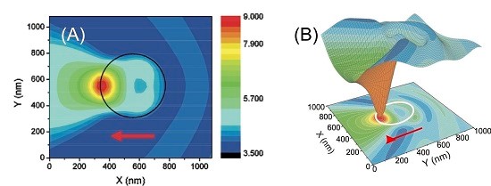
Figure 4: Example of calculation of an energy map resulting from an optical coupling between a latex microbead and a gold disk (A) color map with a scale in meV; (B) corresponding 3D representation [4].
[4] M. Righini et al, Nat. Phys. 3, 477-480 (2007).
Recent studies have shown that it is possible to use surface plasmons to generate heat sources whose intensity is tunable by the excitation wavelength. We have designed new versatile analytical and numerical methods for the three-dimensional calculation of the temperature rise in the vicinity of coplanar plasmonic structures. The formalism allows to reach any illumination shape and is also suitable for the description of near-field polarization effects. A wide variety of geometries can be studied with this technique. In the study presented in Fig. 5, we focused on a periodic array of elongated metallic particles that support one transverse and one longitudinal plasmon mode. In this configuration, we have shown a simple control of the temperature rise in the surrounding medium when the incident linear polarization is rotated. A realistic description of these localized dissipation effects is directly related to a correct description of the imaginary part of the dynamic response function of the nanostructures as well as the distribution of the electric field intensity inside the metal. The total power dissipated by the structure is then calculated after integration of this quantity over the entire metal volume occupied by the metal parts of the device.

Figure 5: Simulation of three temperature maps computed above a set of nine cylindrical gold nano-sticks (25 x 80 nm) illuminated at normal incidence by a linearly polarized plane wave. The wavelength is fixed at 680 nm, close to the center of the longitudinal plasmon band. (A) sample geometry; (B) to (D) evolution of the temperature map as a function of incident polarization.
[5] C. Girard et al, J. Opt. 20, 075004 (2018).
Ohmic losses in plasmonic structures have always been considered as a major shortcoming for long distance propagation and the development of efficient devices. However, the possibility to control the temperature increase through illumination parameters (wavelength, polarization) has triggered a strong interest in the NanoOptics community [1]. This photo-thermal energy conversion originates from the strong local field enhancement associated with the plasmon resonance as well as the amplified absorption in the metal. Metal nanostructures can therefore increase the temperature in their environment and can be used as integrated nano-heat sources [2]. This field of research, thermoplasmonics, could potentially lead to breakthroughs in various fields such as nanomedicine, nanochemistry, or thermally assisted optical manipulation and trapping.
Contact: Christian Girard

Figure 1: Calculated spectra of heat generated in metallic structures deposited on a substrate. The surrounding medium is water. Adapted from reference [1]. ©CEMES-CNRS
Very recently, plasmonics has generated a new field of applications in which dissipative effects in metal are used to advantage. Besides their well-known properties of electromagnetic field exaltation and confinement in the near field, metallic nanostructures and particles have revealed a great potential as local heat sources. This activity is developed at the experimental level (including local temperature measurements by local spectroscopy) and at the theoretical level with a fully self-consistent approach based on the Dyadic Green’s Function (DGF) formalism that allows to calculate the local field strength and temperature distribution in and around a particle lattice (while including the coupling to the substrate).

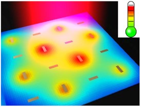
Figure 2: (a) Example of a thermoplasmonic metasurface capable of generating strong temperature contrasts. (b-e) Evolution of the temperature maps as a function of the incident polarization (double arrow) [4]. ©CEMES-CNRS
This approach has been applied to define and optimize new concepts of thermoplasmonic metasurfaces composed of gold nano-rectangles or with a mixture of gold and silicon rods [3,4]. At each step of the optimization, the heat distribution was calculated, and the arrangements restoring a behavior closest to the set objectives were selected. This iterative approach has, for example, converged towards geometries of meta-surfaces optimized for energy transport and capable of generating remote temperature increases, controllable at a distance thanks to the polarization and the wavelength of the laser, thus meeting the objectives set at the beginning.

Figure 3: (a) Diagram illustrating the evolutionary optimization. (b) Top: illustration of the optimization model. An optimized chain of 20 rods on a glass substrate is sought to obtain the maximum temperature rise at one end. Bottom: temperature map along the optimized chain, with expanded views at the launch and end point. Temperatures are calculated at a height of 300 nm (scale bar: 500 nm) [4]. ©CEMES-CNRS
[1] G. Baffou et al, App. Phys. Lett. 94, 153109 (2009).
[2] S. Viarbitskaya et al, ACS Photon. 2, 744 (2015).
[3] P. R. Wiecha et al, Phys. Rev. B 96 (3), 035440 (2017).
[4] C. Girard et al, J. Opt. 20, 075004 (2018).

Doped semiconductors represent a new type of plasmonic material with optical resonances in the infrared. Unlike noble metals, the carrier density in semiconductors, and therefore the plasmon resonance frequency, is tunable. Moreover, due to the characteristics of their band structure, new plasmonic properties are expected, such as the appearance of non-reciprocal plasmons in transition metal dichalcogenides or the lifting of degeneracy of plasmonic modes related to transverse and longitudinal electrons in silicon.
Arnaud Arbouet, Caroline Bonafos, Jesse Groenen, Vincent Paillard and Jean-Marie Poumirol
Contact: Jean-Marie Poumirol
The appearance of localized surface plasmon resonances in ordered arrays of doped silicon nanodisks allows to extend plasmonics to the infrared range. The resonance frequency is simply adjusted with the amount of dopants. Previously limited to noble metals, plasmonic antennas are now made of silicon, a non-toxic and abundant material. These results are essential for molecule detection or thermal imaging. We have used two types of methods to fabricate these nanostructures.
The first one is a top down approach which consists in optimizing the doping of thin layers of silicon on insulator (here SiO2) beyond the usual doses by means of a thermal annealing with a pulsed laser, before forming dense hexagonal arrays of identical disks of nanometric sizes by electron lithography (Fig. 1 (a)). This study was conducted in collaboration with LAAS-CNRS and CEA-LETI, in the framework of the ANR DONNA (Doping at the nanoscale).
These doped nanostructures show intense localized surface plasmon resonances, measured in the mid- and near-infrared by Fourier transform infrared spectroscopy. The plasmon resonance is tunable in a wide spectral window by adjusting the free carrier concentration via phosphorus doping (Fig. 1(b)). Numerical simulations have allowed to study the optical properties of a single nanodisk as well as the metasurface and to identify collective effects and near field coupling in the metasurface.

Figure 1: (a) TEM image in slice view of the doped Si nanodisc array; (b) FTIR (reflectivity) measurement of localized surface plasmon resonances. In insert, evolution of the plasmon resonance frequency as a function of the carrier density.
The second is a bottom-up approach which consists in fabricating Si nanocrystals (SiNCs) by ion synthesis (low energy ion implantation) in a silica matrix and doping them by phosphorus co-implantation. In these cases, small nanocrystals, with radii ranging from 2.6 to 5.5 nm, are formed and randomly organized within the silica matrix (Fig. 2(a)).
Using localized surface plasmon resonance as an optical probe, we revealed the presence of free carriers in these small doped SiNCs. Infrared spectroscopy study coupled with numerical simulations allows us to determine the number of electrically active phosphorus atoms with an accuracy of a few atoms. We have shown that plasmon resonances can be supported with only about ten free electrons per nanocrystal (Fig. 2(b)) confirming theoretical predictions and probing the limit of the collective nature of plasmons. We demonstrated a strong coupling (hybridization) between the surface plasmon resonance localized in the doped nanocrystals and the phonons of the silica matrix. Finally, a careful analysis of the dependence of the electron mobility on the carrier density in this small size regime has allowed us to detect the appearance of a new process in the high dopant concentration range, attributed to the precipitation of phosphorus inside the SiNCs.
This work is being carried out in the framework of the ANR DONNA (Doping at the nanoscale, 2018-2022).

Figure 2: (a) Energy-filtered image in wafer view of phosphorus-doped SiNCs (white contrast) embedded in the silica matrix; in insert, high-resolution microscopy image of an individual doped SiNC. (b) Evolution of the number of electrons/NCs as a function of electron density.
These results open very promising perspectives for the development of all-silicon integrated plasmonic devices for applications requiring broadband and high resolution infrared detection, such as micro-integrated bolometers or miniaturized infrared cameras.
The Ti-P project proposes to study the non-reciprocal dispersion of plasmons related to the topological properties of the electronic band structure of Dirac materials and in particular of monolayers of transition metal dichalcogenides. The Berry curvature is a topological property of the electronic band structure present in Dirac materials. It gives rise to a transverse velocity that affects the direction of propagation of charge carriers, causing an accumulation of charges along the edges of the system. This unique property allowed the first observation of a valley Hall effect in optically doped transition metal dichalcogenides. Ti-P is based on the scientific assumption that these phenomena observed by transport measurements will have an optical equivalent: plasmonic modes with non-reciprocal dispersion, i.e. a different dispersion for positive and negative momentum values. The project aims at providing an experimental observation of such a non-reciprocal dispersion of surface polariton plasmons through far field infrared spectroscopy measurements. Ti-P proposes to design plasmonic crystals specifically designed to support non-reciprocal plasmonic modes, through asymmetric valley doping generated using a circularly polarized (in the visible) optical pump and through infrared spectroscopy measurements to characterize changes in the polarization state and light interacting with the plasmons. With the observation of these modes, we mainly aim at a better understanding of the impact of the topology on the collective excitations of the charge carriers but also to take the first steps towards the development of a “valleetronic” light control technology.
|
By positioning the metal tip of a scanning tunneling microscope (STM) a few angstroms from the surface of a metallic or semiconductor sample, it is possible to highlight, under certain polarization voltage conditions, a photon emission generated by the polarized tunnel junction. This extremely localized light source allows the study at a nanometric scale of the electromagnetic properties of the tunnel junction and of the inelastic processes of which it is the seat. |
SINanO contact: Roland Coratger
NeO contact: Renaud Péchou
At CEMES, the experimental study of the STM-induced light emission (STM-LE) phenomenon is possible in the laboratory’s clean room. A hybrid near field microscope (AFM-STM-PSTM, see figure below) is equipped with large numerical aperture optical fibers constituting an original system of collection of the emitted photons. These optical fibers are the first link of two distinct measurement chains. The first one, constituted by a cooled photomultiplier operating in photon counting mode in the range 185-900 nm, allows to draw up photon maps (number of photons emitted in each point of the explored area on the sample surface), and the second one consists in a spectrometer equipped with a CCD matrix cooled with liquid nitrogen which allows to access the spectral characteristics of the emitted radiation in the range 300-1050 nm. These experimental data are correlated to the STM images acquired simultaneously.
|
Figure 1: STM/AFM Dimension 3000 and emission spectra obtained on an Au/Au junction © CEMES-CNRS |
The elementary physical mechanisms responsible for this emission depend on the type of sample studied: radiative de-excitation of localized plasmon modes excited by inelastic tunnel electrons in the case of metal-metal junctions, and radiative electron-hole recombination in the case of metal-semiconductor junctions.
The STM stimulated light emission is complementary to other more classical near field analysis techniques developed in the laboratory, such as STM or optical near field. It allows the study of fundamental physical properties (e.g. the plasmonic density of states) on nanostructures or assemblies of metallic nanostructures (rods, prisms, sub-wavelength waveguides). It can also be relevant to study the effects of coupling between these nanostructures and the appearance of hybrid modes. It is also used to study the luminescence of two-dimensional semiconductors (such as transition metal dichalcogenides (TMD) for example) locally excited by tunneling electrons.
Equipment used: STM Dimension 3000, cooled Hamamatsu PM, cooled Princeton CCD Spectroscope LN2.
Collaborations: LAAS-CNRS (Pr. A. Mlayah), Rice University (Pr. J. Lou), University of Texas at San Antonio (Dr. N. Large), mechanical part of the Engineering Pole of CEMES.
[1] R. Péchou et al, Appl. Phys. Lett. 72, 671 (1998).
[2] A. Carladous et al, Phys. Rev. B 66, 045401 (2002).
[3] C. Maurel et al, Surf. Sci. 600, 442 (2006).
[4] R. Péchou et al, ACS Photonics, 7, 3061 (2020).
(no text for the moment)…
The FemTOTEM project aims at developing an ultrafast transmission electron microscope (UTEM) based on a high brightness laser driven field emission electron source. This will be achieved by combining a femtosecond laser source and a custom cold field emission transmission electron microscope (CFEG-TEM). This combination of femtosecond time resolution, high brightness (allowing high spatial resolution and electron coherence) and energy resolution will have unique potential for cutting edge research in nanophysics and materials science.
The first part of this project concerns instrumental developments. First, we will demonstrate and characterize laser-driven field emission from the custom electron source of a commercial 200kV TEM. The femtosecond cold field emission gun that we have already mounted on a dedicated ultra-high vacuum (UHV) bench will be fully characterized in terms of emitted current and energy spectrum as a function of laser parameters and extraction voltage. Then, it will be transferred to a TEM column. Its potential for electron microscopy experiments will be studied in depth, first on routine TEM applications, then on more demanding experiments. A new accessory allowing the injection and collection of light on the TEM sample, already designed, will allow us to perform original experiments involving electrons and photons. The principle of an ultrafast TEM is illustrated in the figure below. An ultra-short laser pulse excites the sample inside the objective lens. A second laser pulse, delayed, triggers the emission of ultra-short electronic pulses inside the electron microscope.

This project involves two CEMES research groups (I3EM and NeO) and is a collaboration between CEMES and LPS-Orsay (Mathieu Kociak).
Financial support:
The FemtoTEM project is supported by the Institut de Physique du CNRS and the Agence Nationale de la Recherche (grant ANR-14-CE26-0013, 2014-2018).
Contacts: Arnaud Arbouet & Hugo Lourenço-Martins
(no text for the moment)…

In noble metal nanostructures, the interactions between light and electronic and vibrational excitations are largely modified compared to what happens in bulk materials. Their sizes are significantly smaller than the wavelength of light, skin depth, electron mean free path, acoustic wavelength… The resulting confinement and damping effects on the dynamics of collective or individual, atomic or electronic vibrations have been analyzed by resonant Raman scattering of plasmons under specific experimental conditions on a panel of multilayer composite samples. On the one hand, we show that the so-called “background” in SERS is an intrinsic phenomenon due to inelastic scattering by electronic excitations. Its increase, the shape of the spectral lines and the size dependence are well explained by the application of a dirty metal model, developed at the beginning to describe the electronic scattering in superconductors. On the other hand, we show experimentally, for the first time, that the density of vibrational states is modified when the surface-to-volume atomic ratio is reduced (the 3D-2D transition), leading to thermodynamic anomalies. These fundamental studies are of primary importance for the understanding of the SERS phenomenon, but also for various applications, such as photo-catalysis and thermo-plasmonics.
Contact: Robert Carles

References:
– Plasmon-resonant Raman spectroscopy in metallic nanoparticles: Surface-enhanced scattering by electronic excitation. R Carles, M Bayle, P Benzo, G Benassayag, C Bonafos, G Cacciato, V. Privitera . Phys. Rev. B 92 (17), 174302, 2015
– Enhancing carrier generation in TiO2 by a synergistic effect between plasmon resonance in Ag nanoparticles and optical interference. G. Cacciato – M. Bayle – A. Pugliara – C. Bonafos – M. Zimbone – V. Privitera – MG. Grimaldi – R. Carles. Nanoscale, 7, 13468-13476 (2015)
– Experimental investigation of the vibrational density of states and electronic excitations in metallic nanocrystals, M Bayle, P Benzo, N Combe, C Gatel, C Bonafos, G Benassayag, R. Carles. Phys. Rev. B 89 (19), 195402, 2014
– Vibrational and electronic excitations in gold nanocrystals. M Bayle, N Combe, NM Sangeetha, G Viau, R Carles. Nanoscale 6 (15), 9157-9165, 2014
– Vibrational density of states and thermodynamics at the nanoscale: the 3D-2D transition in gold nanostructures, R. Carles, P. Benzo, B. Pécassou and C. Bonafos. Scientific Reports 6, 39164 (2016)
DIMENSION: TransitioN MEtals DIchalcogenides: Synthesis and applicatiONs
Occitanie Research and Society Project 2019-2023

Jean-Baptiste Dory et al 2022 Mater. Res. Express 9 045006
https://doi.org/10.1088/2053-1591/ac5273
The main objective of the project is to design new optoelectronic devices based on highly absorbing 2D materials (MoS2) combined with photonic nanostructures. The study of the optical properties of 2D materials and their exploitation in innovative devices is an exciting and fast growing research field, motivated by fundamental science and by applications in various fields (energy production and storage, biochemical detection…).
The discovery of surface plasmon resonances (LSPR) in doped semiconductor nanocrystals has opened the way to a new regime in plasmonics. Nevertheless, there is no clear vision of the insertion and activation of dopants and no efficient doping process at the nanoscale. The goal of the DONNA project is to develop new approaches for efficient doping of Si-NCs, involving non-equilibrium processes. Model systems consisting of monodisperse Si-NCs will be fabricated by different physical methods coupled with laser annealing for efficient dopant activation. Atomic mapping of the dopants will be obtained by STEM-EDS and atomic probing while the LSPRs generated in these doped NCs will be used as optical probes to measure their activation. This fundamental project (TRL1) involving academic laboratories (CNRS and CEA) and an SME will pave the way for active, reconfigurable and CMOS compatible plasmonics.
The 2DLight project concerns the study of the optical properties of 2D materials based on transition metal dichalcogenides. The focus is on the optimization of the light emission and its directivity by coupling the TMD monolayer to dielectric nano-antennas. The influence of different parameters (near field enhancement, local photon density of states, deformation of the layer, etc.) is taken into account.
The HiLight project aims at developing efficient, broadband, integrated nanoscale light sources operating at room temperature and covering the visible and infrared spectra. The light sources are formed by quantum emitters positioned in the optical near-field of high index dielectric nano-antennas.
NAMAS: PHOTOCONDUCTANCE OF GOLD NANOPARTICLE ASSEMBLIES: FROM TO NANO- TO MACRO-SCALE
Project NanoX Namas 2021-2024
The project focuses on a research topic at the interface of charge carrier transport and optical properties of hybrid nano-structures composed of self-assembled metal nanoparticles. The main objective of the project is to study both experimentally and theoretically the fundamental mechanisms of photocurrent generation by optical excitation of surface plasmons supported by interacting metal nanoparticles. An ambitious goal of the project is to bridge the gap between local phenomena (localized surface plasmons, electron tunneling, molecule/metal state hybridization) and meso/macroscopic effects (percolation, structural disorder, size and distance fluctuations) involving the whole nanoparticle assembly.

Animal coloring is an interdisciplinary field that has attracted increasing interest over the last 20 years, but despite the efforts, many questions remain open. The structures that produce colors are often very complex. Natural selection is responsible for structures that not only have extraordinary optical properties, but are also multifunctional. Indeed, natural structures are the result of millions of years of research and development, and their knowledge should have a strong impact on future developments in several disciplines including optics. Color is an essential aspect of the physiology and functional morphology of integuments. One of the key questions in the color theme is how nanostructures are used to shape light. This project is specifically concerned with how nanostructures (including or not pigments) produce color. Two different cases are studied in a first step, in collaboration with colleagues from the EDB (Ecology and Biological Diversity) laboratory in Toulouse: ladybugs and common lizards. Other species will then be studied according to our results.
ANR – QUantum free Electrons for NaNOopTics – QUENOT
The ambition of QUENOT is to overcome several current conceptual and experimental limits in nanooptics by using the quantum properties of fast electrons. Indeed, some key concepts and quantities in nanooptics (super-chirality, spatial coherence of excitations in optical nanostructures and quantum optics of photonic excitations) have been very little studied at their relevant scale: the sub-wavelength scale. The founding idea of QUENOT is that the quantum properties of fast electrons, long considered difficult to manipulate from a theoretical and experimental point of view, allow the measurement of super-chirality, CDOS, as well as the preparation and measurement of Fock states in photonic nanostructures at the nanoscale.
We intend to address these conceptual and technical challenges through a consortium combining theoretical and experimental expertise in nano-optics, advanced nanofabrication and electron optics instrumentation.
Link to the project description:
https://anr.fr/Project-ANR-20-CE30-0033
PROJECT COORDINATOR
Mr Mathieu KOCIAK (Solid State Physics Laboratory)
The author of this summary is the project coordinator, who is responsible for the content of this summary. The ANR declines any responsibility as for its contents.
PARTNERS
CEMES CENTER D’ELABORATION DE MATERIAUX ET D’ETUDES STRUCTURALES
UPSACLAY – C2N Center for Nanoscience and Nanotechnology
L2n Light, nanomaterials, nanotechnologies – CNRS ERL7004
LPS Laboratoire de Physique des Solides
Interaction of biological targets with dielectric thin films containing silver nanoparticles: towards tunable antimicrobial surfaces
The BENDIS project aims at exploiting in an original way the antimicrobial properties of silver nanoparticles (AgNPs) buried in a silica matrix. Our ambition is to develop “nano-safer by design” systems, intended to ensure a controlled antimicrobial activity of AgNPs. The objectives of BENDIS are: (i) to identify the key mechanisms responsible for protein adhesion on these dielectric surfaces, (ii) to evaluate the role of proteins in cell adhesion, (iii) to reveal how silica-embedded AgNPs modify protein/cell adhesion and biofilm formation by Ag+ and/or AgNPs release and (iv) to evaluate the controlled antimicrobial efficacy of these coatings. The results obtained should give an impulse to the design of adjustable antimicrobial surfaces, with low sanitary and environmental impacts, for applications in the health field via the control of biocontaminations.
The Ti-P project proposes to study the non-reciprocal dispersion of plasmons related to the topological properties of the electronic band structure of Dirac materials and in particular of transition metal dichalcogenide monolayers. The Berry curvature is a topological property of the electronic band structure present in Dirac materials. It gives rise to a transverse velocity that affects the direction of propagation of charge carriers, causing charge accumulation along the edges of the system. This unique property allowed the first observation of a valley Hall effect in optically doped transition metal dichalcogenides. Ti-P is based on the scientific assumption that these phenomena observed by transport measurements will have an optical equivalent: plasmonic modes with non-reciprocal dispersion, i.e. a different dispersion for positive and negative momentum values. The project aims at providing an experimental observation of such a non-reciprocal dispersion of surface polariton plasmons through far field infrared spectroscopy measurements. Ti-P proposes to design plasmonic crystals specifically designed to support non-reciprocal plasmonic modes, asymmetric valley doping generated using a circularly polarized optical pump (in the visible) and infrared spectroscopy measurements to characterize changes in the polarization state and light interacting with the plasmons. With the observation of these modes, we mainly aim at a better understanding of the impact of the topology on the collective excitations of the charge carriers but also to take the first steps towards the development of a valleetronic light control technology.