Our fields of activity:
– Classical preparation for TEM (thin section) and SEM (scanning electron microscopy)
– FIB preparation of localized thin sections
– Multi-scale imaging (Optical, SEM, TEM, HRTEM)
– Orientation and chemical mapping (EDSD, ASTAR, EDS, EELS)
Our strengths:
– Expertise in mechanical, electrolytic and ionic thinning
– Expertise in imaging, spectroscopy, diffraction
– Wide range of TEM holders for in situ observations (temperature, traction, multi-contact, …)
– Maintenance and training on all the department’s equipment
– External services (local, national, European…)
The sample preparation department is the essential activity that precedes electron microscopy observation. Conventional methods consist of surface polishing for scanning electron microscopy (SEM) observations, or thinning the samples to a few tens of nanometres thick for transmission electron microscopy (TEM) observations. However, sample preparation can become more exotic depending on the problem at hand.
The department provides the laboratory with numerous tools and different preparation techniques, which are taught to students and those wishing to be trained.
Whether conventional or more modern, sample preparation requires great precision, skill and patience on the part of the operator!
This department is composed of two members Catherine Crestou TCE CNRS (specialist in ion thinning) and Dominique Lamirault TCN ITRF (specialist in electrolytic jet thinning)

Ion beam thinning: GATAN PIPS Model 691

Plane view of a BaTiO3 sample

Cross-section of a BaTiO3 sample

Electrolytic jet thinning: STRUERS TenuPol-5

Sample of a metal alloy on a copper grid
Cutting tools :

ONA AF25 wire EDM machine

ESCIL Well diamond wire saws

BUEHLER IsoMet 4000 saw
Mechanical thinning :

ESCIL 300GTL, 200GTL polishers

ALLIED Multiprep semi-automatic polisher

BUEHLER Phoenix 4000 polisher

BUEHLER vibratory polisher

VibroMet2 GATAN Grinder

SOUTH BAY TECHNOLOGY Tripod Polisher Model 590

GATAN Dimpler Grinder Model 656
The FIB/SEM dual beam systems consist of two microscopes: a SEM (Scanning Electron Microscope) column and a FIB (Focused Ion Beam) column. They allow the observation and abrasion of matter at the scale of ten nanometres. They can also accommodate numerous other pieces of equipment for depositing material (Pt, W, Au, C), moving objects or performing chemical or crystallographic analysis, always on a submicrometre scale.
We use these machines at CEMES to carry out numerous experiments on all types of materials: preparation of thin slides for transmission electron microscopy (TEM), EDS and EBSD analyses, etching of pillars and beams for in situ compression and bending tests, etching of stencil gratings on Si3N4 membranes, electrical contact by localised metal deposition, etc.
This department is composed of one person: Robin Cours, CNRS Research Engineer.
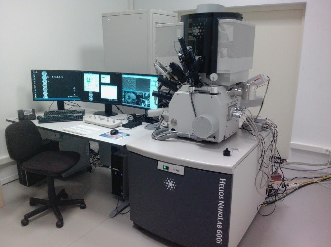
Helios NanoLab600i
Strengths: TEM thin foil preparation, EDS EBSD, MEB FEG analysis
Microscope Helios

Microscope Helios NanoLab600i
Zeiss CrossBeam 1540 XB
Strenghts: Electron lithography, SEM FEG

Microscope Zeiss CrossBeam 1540

Installation of a carbon nanocone on an AFM cantilever head
Transmission electron microscopes (TEM) consist of an electron gun (source), electromagnetic lenses that act on the electron beam and various detectors. These detectors allow images to be obtained, diffraction images that provide information on the shape and structure of the sample, but also on its chemical composition or its mechanical, magnetic or electrical properties…. TEMs allow very local observation of materials (from a few µm2 to a few Å2). For the electron beam to pass through the sample, the latter must be very fine (of the order of 100nm).
There are 6 TEMs available for internal or external users at CEMES, 4 conventional (CM20, JEM2010, CM20FEG, HF2000) and 2 corrected for image mode aberrations (TECNAIF20 and HF3300 I2TEM). A very wide range of sample holders is also proposed in order to act in-situ (i.e. in the microscope) on the materials studied. It is then possible to orientate, heat, deform and apply fields to our samples in order to determine their intrinsic properties.
The department provides training for users who wish to become autonomous in all the techniques offered by the park (conventional imaging, parallel mode and precession diffraction, ASTAR, high resolution, STEM, EELS/EDX spectroscopy, EFTEM, etc.), and provides services in one of the techniques mentioned above.
The department is composed of two members: Sébastien Joulié, CNRS engineer in charge of the CM20, JEM2010 and TECNAIF20 microscopes, and Cécile Marcelot, CNRS engineer in charge of the CM20FEG, HF200 and I2TEM microscopes.
CM20 (200kV)

Microscope CM20

Cobalt nano wires
JEOL 2010 (200kV)
Strengths: dark field, in situ video

Microscope JEOL 2010

Dislocations in a nickel-base superalloy
CM20 FEG
Strengths: EDX spectroscopy, Astar precession

Microscope CM20 FEG

EDX mapping of a Al-Cu alloy

Orientation mapping of an iron oxide dendrite
TECNAI F20 (200kV)
Strengths: high resolution, EELS spectroscopy

Microscope Tecnai F20

Fe3O4 nanoparticle
HF2000 (200kV)

Microscope HF2000

Growing of nano wires of Co on Al2O3
I2TEM (HF3300) 300kV
Strengths: electron holography, in operando, high resolution, EELS spectroscopy

Microscope I2TEM (HF3300)

Hologram on a CoFe2O4 nano flower
The optics and magnetism department brings together all the laboratory’s experimental capabilities in optics and magnetism. It provides users inside and outside the laboratory with tools for characterising the optical/magnetic properties of materials. The optical part includes near- and far-field Raman spectroscopy devices as well as temporal measurement capabilities from femtosecond to millisecond. Spatial mapping of the properties measured on structured samples is available on all devices. The magnetism section includes macro- and microscopic Kerr magneto-optical, radio-frequency and magneto-transport measurements under cryostat.
The service’s devices are either directly accessible by users (after training) or in collaboration with the researchers who “set up” the device.
Sébastien Moyano, Frédéric Neumayer, Sébastien Weber (leader)

Atomic Force Microscope coupled to a Raman spectrometer constituting our TERS (Tip Enhanced Raman Spectrometer)
– Spectral analysis in reflectance, fluorescence and Raman emission
– UV, visible and near infrared analysis
– Micrometer resolution hyper-spectral mapping
– Nano tip excitation spectrometry: 10/20 nm resolution spectro-spatial mapping
– Fluorescence lifetime mapping: micrometer resolution and >100 picoseconds
– Pump-probe measurements of femtosecond/picosecond dynamics
– Non-linear microscopy
– Quantum plasmonics: single photon counting (intensity time correlation)
– Ultrafast Transmission Electron Microscopy, stationary and time-resolved cathodoluminescence (joint CNRS Hitachi laboratory: HC-IUMI)
– Broadband ferromagnetic resonance measurements (0-20 GHz) in stripline configuration
– Spin dynamics measurements on micro-antennas, by synchronous detection (field modulation), vector analysis (network analyser) or spectral analysis (spectrum analyser).
– Magnetometry and magneto-transport 0 – 9T, 2 – 400 K.
Strenghts:

Functional diagram of the PyMoDAQ library for the control of experimental devices and data acquisition

a) Micro-MOKE: Device for characterising magnetisation under a microscope using the MOKE (Magneto-optical Kerr Effect).
b) Image of magnetic domains acquired using the Micro-MOKE and its software under PyMoDAQ.
The department has different types of lasers (continuous, pulsed, gas, solid-state…) used on the different experimental devices according to the needs as well as lasers attached to particular devices:
– Continuous, fixed and fibre-coupled lasers:
◦ Krypton [406-676 nm] emission on atomic lines
◦ Argon [457-514 nm] emission on atomic lines
◦ Titanium: Sapphire [700-1050 nm] tunable emission

Optical table (Spectro T64000) with a set of gas LASERs (Argon, Krypton and solid-state: Ti-Sa). These sources can be delivered to the different experimental rooms by optical fibre.
– Mobile lasers:
◦ Super-continuum [450-2500 nm], [250-40000 kHz]
◦ DPSS diode @488nm
◦ Diode Continuous or pulsed lasers (20 picoseconds):
▪ Aurea: 405nm, 632nm, 785nm
▪ PicoQuant: 532nm, …
◦ Helium Neon
◦ …
– Horiba/Jobin Yvon T64000 Spectrometer. The most versatile spectrometer:
Single monochromator or triple monochromator
Near UV and visible range
Arrays: 2400, 1800 and 150 rpm
– Dilor UV Spectrometer
Triple monochromator
Laser: Ar [275-364 nm]
Array: 2400 rpm
– X-Plora Horiba/Jobin Yvon. The most used spectrometer
Lasers: DPSS @ 532 nm, diode lasers @ 638 and 785 nm
Arrays 2400, 1800, 600 and 300 rpm
Reflection and transmission white lamps
– TERS: Tip Enhanced Raman Spectrometer. Coupling of a LABRAM spectrometer, a TRIOS AFM and silver tips
DPSS laser at 532nm and He:Ne at 632nm
1800 and 300tr/mm gratings
– FLIM: Fluorescence Life-time Imaging Spectrometer
Uses pulsed diode lasers or fibre gas lasers
Micrometric spatial and temporal resolution greater than 20 picoseconds
Hyper-spectral or hyper-temporal mapping
– Femtosecond bench
Coherent Chameleon Ultra II femtosecond oscillator, 80 MHz, 100 fs, 680-1080 nm
Frequency doubler/tripler
Femtosecond time probe pump measurements in transmission or reflection
Micrometric spatial resolution
– FemtoTEM ultrafast electron microscope:
Amplified femtosecond laser source Amplitude Satsuma systems, single shot to MHz, 20 uJ/pulse, 250 fs
Electron imaging, EELS spectrum and time-resolved cathodoluminescence
The Characterisation Department brings together several complementary activities with a single aim: to offer a multidisciplinary approach to the characterisation of materials. It has a very large number of instruments that enable it to explore numerous properties of materials such as those related to their interfaces, morphologies, mechanical or crystallographic characteristics. This equipment is complemented by various means of sample preparation, including a set of high-temperature furnaces (up to 1500°C).
The department offers its skills for both simple measurements and more in-depth studies of many types of materials, sometimes requiring instrumental and/or methodological development.
It relies on the specific skills of its staff members: David Neumeyer, for granular materials and their characterizations, Christophe Deshayes for mechanical tests and scanning electron microscopy observations. The X-ray diffraction activity completes and extends the department’s means of investigation.
A large part of the department’s equipment is accessible to users after theoretical and practical training in the techniques and interpretation of the results.
Contact : david.neumeyer@cemes.fr

Some examples of available means and results: a-1 and a-2 Brucker Discover Diffractometer (2D), example of result obtained for an ancient Chinese pottery shard paste (Clément Hole) b-1 measured mesoporosity and c-1 to 3, Malvern NanoZS, Zeta potential and Phase Plot (Commercial Alumina – CE NanoDesk)