In situ biasing electron holography of hafnia-zirconia device
January 6, 2026
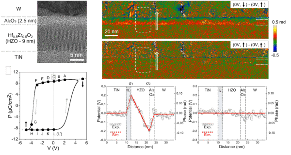
In this work, we demonstrate how operando electron holography can be used to directly map the internal electric fields and interface charges in a Hf0.5Z0.5O2 tunnel junction. Polarization switching is observed across large areas and shown to proceed via domain nucleation and lateral growth, providing quantitative insight into charge screening and interface engineering in ferroelectric devices.
Understanding charge screening and polarization switching is essential for optimizing hafnia-based ferroelectric devices. Yet, direct experimental access to internal electric fields and trapped charges has remained elusive. Here, we demonstrate that operando electron holography enables quantitative mapping of electric fields and charge densities within a W/ Hf0.5Z0.5O2 / Al2O3 / W tunnel junction.
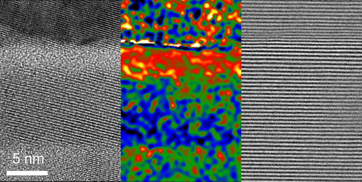
By electrically biasing the device inside the transmission electron microscope, we measured the electrostatic phase shifts associated with different polarization states while eliminating static contributions such as mean inner potential. This differential approach allows direct visualization of polarization reversal over a ~300 nm field of view. We show that polarization switching occurs through both nucleation of reversed domains and their lateral growth as the applied voltage approaches the coercive field.
Quantitative analysis revealed that screening charges are predominantly localized at ferroelectric/dielectric interfaces and that unintended interfacial layers significantly modify the internal electric field profile. The average electric field in the ferroelectric layer was measured with an accuracy of 0.02 MV·cm-1, while local field variations and interface charge densities are resolved with sub-nanometer spatial resolution.
This work establishes operando electron holography as a powerful tool bridging macroscopic electrical measurements and atomic-scale structural analysis. By providing direct access to internal electric fields and charge screening mechanisms, it opens new pathways for interface engineering and performance optimization of nanoscale ferroelectric devices.
Contacts:
Christophe Gatel | christophe.gatel[at]cemes.fr
Martin Hÿtch | martin.hytch[at]cemes.fr
Publication:
Mapping electric fields and observation of ferroelectric domain switching in hafnia-zirconia devices by electron holography
L. Zhang, C. Gatel, M.H. Raza, K. Gruel, C. Dubourdieu, and M.J. Hÿtch
Nature Communications 16, 11233 (2025)
DOI: https://doi.org/10.1038/s41467-025-66807-4
-
Previous Post
Bertrand Gatti
Related Posts
The capabilities of a microscope revealed by Fourier
March 19, 2026 Seminar by Emmanuel Soubiés, CNRS researcher at IRIT, Toulouse Open to all