Towards the next generation of quantum sensors
October 3, 2023
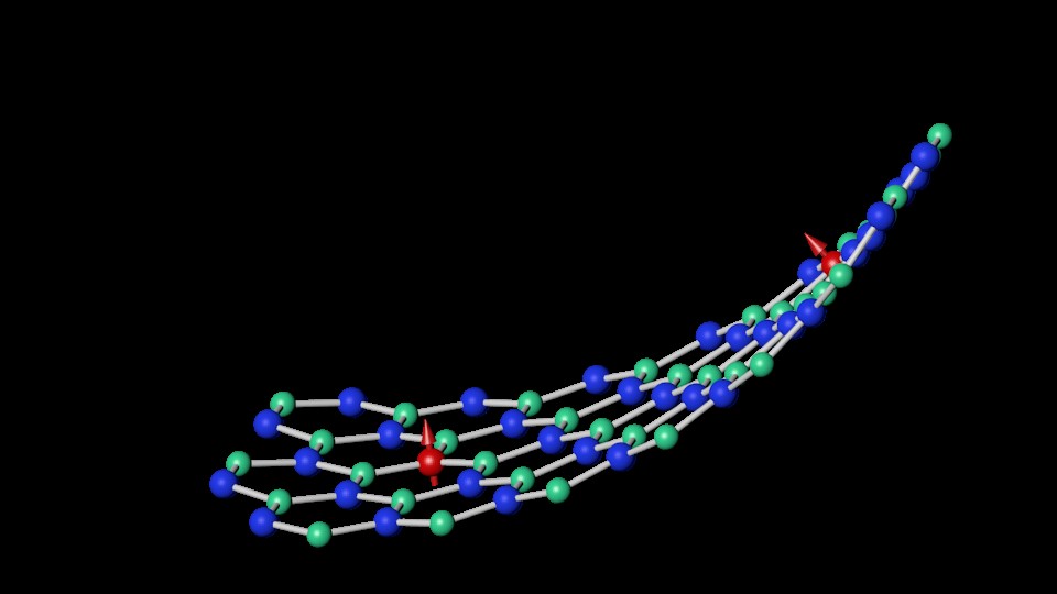
The negatively-charged boron-vacancy (VB–) center in hexagonal boron nitride (hBN), created by ion implantation at Cemes, is promising for developing 2D spin-based quantum technologies. The electronic spin resonances of this point defect strongly depend on external perturbations (electric and magnetic fields, temperature) and can be controlled optically under ambient conditions even in the limit of atomic hBN layers, offering new prospects for quantum sensing with unprecedented proximity to the sample.
Quantum sensing technologies powered by solid-state spin defects have already shown a huge potential for covering the growing need for high-precision sensor. However, sensing methods based on spin defects in 3D materials, such as NV centers in diamond, are limited in spatial resolution due to the impossibility to engineer ultrathin and flexible sensors that could be as close as possible to the sample. Spin defects in atomically-thin 2D materials, like VB– centers in hBN, overcome these limitations.
To maximize the sensing performance of VB– centers, isotopically-purified hBN crystals were studied by Electron Spin Resonance (ESR) of VB– centers. Boron has two stable isotopes, 11B (80% natural abundance (na)) and 10B (20% na), while nitrogen occurs as either 14N (99.6% na) or 15N (0.4% na). In hBN crystals with natural isotopic content (h11B14N), when applying a weak static magnetic field Bz that splits the electron spin sublevels (Zeeman effect), the ESR of VB– centers is characterized by a complex seven-line structure resulting from the hyperfine interaction with the three 14N nuclei placed in the first neighboring lattice sites. The hyperfine coupling with the second-neighbors boron atoms rather leads to an overall broadening of each ESR line. The other isotopic configurations of hBN (h10B14N, h10B15N, and h11B15N) were then studied in the same way.
This work shows that isotopic purification with 15N yields a simplified and well-resolved hyperfine structure of VB– centers, while purification with 10B leads to narrower ESR linewidths (see Figure). These results establish isotopically-purified h10B15N crystals as the optimal host material for future use of VB– spin defects in quantum technologies.
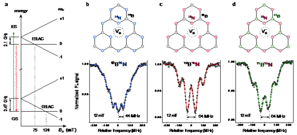
Figure – (a) Simplified energy level structure of the VB– center in hBN showing the electron spin sublevels ms = 0,±1 in the ground (GS) and excited states (ES), as well as their evolution with a static magnetic field Bz applied along the c-axis of hBN. Hyperfine structure of the VB– center in (b) h10B14N, (c) h10B15N, and (d) h11B15N crystals.
The next step now is to reduce the thickness of the hBN layer to achieve ultimate atomic-scale proximity between the sensor and the probed sample.
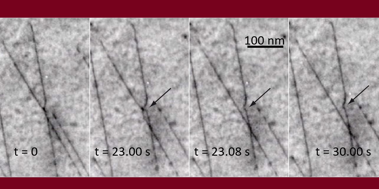
Cemes (MEM team and ATP platform) is involved in these promising developments by creating the VB– defects by ion implantation as an alternative technique to neutron irradiation, which main drawbacks are accessibility and potential hazard due to transmutation products. However, using ion implantation requires optimizing the ion/energy/dose combinations to create dense array of VB centers in ultrathin hBN flakes ideally down to the monolayer limit. This will be done by:
– advanced Monte Carlo simulations to select implantation parameters that optimize VB center formation.
– performing wide range of ion implantations on exfoliated hBN flakes of various thicknesses.
– high-resolution transmission electron microscopy to measure VB center density.
This work is supported by:
– ANR QFoil (L2C, LPCNO, Cemes)
– NanoX Q2D-Sens (LPCNO, Cemes)
Publication:
Isotopic control of the boron-vacancy spin defect in hexagonal boron nitride
T. Clua-Provost, A. Durand, Z. Mu, T. Rastoin, J. Fraunié, E. Janzen, H. Schutte, J. H. Edgar, G. Seine, A. Claverie, X. Marie, C. Robert, B. Gil, G. Cassabois, V. Jacques
Physical Review Letters 131 (2023) 126901
https://doi.org/10.1103/PhysRevLett.131.126901
Contacts:
Alain Claverie | alain.claverie[at]cemes.fr
Grégory Seine | gregory.seine[at]cemes.fr
-
Previous Post
Assya Boughrara
-
Next Post
Romain Gautier