Studying the active area of an individual device in operation
May 7, 2024
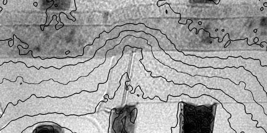
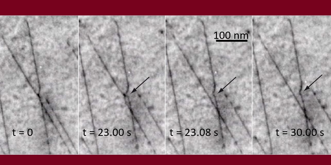
A new method based on operando electron holography was developed to map the resistivity at the nanoscale across the active area of a working individual device. This method has been applied on a phase change memory cell in wall architecture and directly highlighted unexpected features. On switching the memory state by electrical pulses inside the TEM, we studied the resulting electric field and demonstrated that electrical resistance is inhomogeneous near the heater.
The use of electrical resistivity as a parameter to drive devices is receiving increasing attention due to the development of memristors, resistive random-access memory (RRAM) and phase-change memories (PCM). Applications range from active components for more energy-efficient machine learning and in-memory computing to emerging photonic applications. Additionally, PCM promise better performance and a strong interest for low-energy applications.
Phase-change materials such as GST materials exhibit a huge change of electrical resistivity between the amorphous (high resistance) and crystalline phase (low resistance). To read the device, the resistance is measured by biasing the top and bottom electrode connected to a thin metallic filament called the “heater”. To write, a high-amplitude current pulse is injected, whose exact form depends on whether the operation is to stabilize the crystalline phase (SET) or the amorphous state (RESET). Current passing through the heater and GST layer causes localised Joule heating; the associated rise in temperature in turn causes the phase change. To SET, a relatively long pulse allows gradual crystallisation of the amorphous state whilst for RESET, a short pulse induces rapid melt-quench of the crystalline to amorphous state. Once the current pulse has passed, no power is required to maintain the state.
In order to understand the operation of devices, different in situ techniques have been developed to monitor the phase transition, notably in transmission electron microscopy (TEM). A distinction needs to be made between in situ experiments that heat the whole specimen, usually thin films, to provoke the phase change and operando experiments that aim to be closer to the actual operation of devices by injecting current pulses in situ. However, all depend on structural or chemical analysis and do not probe directly the local electrical properties. Here we present a method based on operando electron holography to determine the local resistance with nanometre spatial resolution. We demonstrate the technique on a working industrial PCM device and reveal the inhomogeneity of the resistivity in the active layer. Beyond the interest for PCM, the technique is applicable to many other devices where changes in local electrical resistance are of primary importance.
Publication:
Measuring electrical resistivity at the nanoscale in phase change materials
Leifeng Zhang, Frédéric Lorut, Kilian Gruel, Martin J. Hÿtch, and Christophe Gatel
Nano Lett. 2024
https://doi.org/10.1021/acs.nanolett.4c01462
Contact:
Christophe Gatel | christophe.gatel[at]cemes.fr
Martin Hÿtch | martin.hytch[at]cemes.fr