Tailoring the Electromagnetic Field at the nanometer scale
November 17, 2026
Combining optical absorption of graphene with optical interference in an ultrathin silicon optical cavity could enable more efficient use of semiconductor material in solar-energy devices.
How can a solar cell make effective use of light while containing only a tiny fraction of the silicon used in conventional devices? One approach is to engineer the optical field rather than relying solely on the thickness of the absorbing semiconductor.
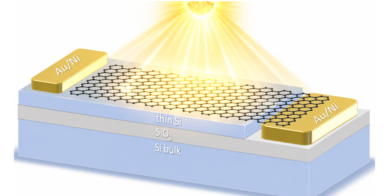
A new device architecture combines graphene, a 100-nanometre-thick silicon layer and a dielectric spacer on a reflecting silicon substrate. Graphene plays a dual role: it provides an ultrathin conductive electrode at the Schottky junction while introducing optical absorption with relatively low reflection. This allows light to interact with the junction without requiring a thick metallic electrode or a thick silicon absorber.
The layered structure also acts as an open optical cavity. Interference between forward- and backward-propagating light waves creates a standing-wave pattern whose maximum can be positioned at the graphene/silicon junction by adjusting the layer thicknesses. The calculations predict an optical-field enhancement factor of 8.4 at a wavelength of 700 nm. By tuning the dielectric spacer, the optical response can be optimized over relevant parts of the visible spectrum.
Reducing the silicon thickness inevitably decreases its total absorption. However, the engineered optical interference can compensate for some of this loss, producing enhanced photocurrent in the ultrathin-device regime.
The modeled comparison illustrates the potential material advantage. A device containing 100 nm of silicon produces a photocurrent of 0.89 mA, compared with 27 mA for a bulk-silicon reference containing 250 μm of silicon. Despite its lower total photocurrent, the ultrathin device achieves a calculated photocurrent per unit silicon thickness that is 82.4 times greater.
Initial experimental devices based on graphene and silicon-on-insulator substrates demonstrate the feasibility of nanometer-thick silicon-based solar-cell structures. Further work on the graphene/silicon interface and electrical contacts is needed to establish and improve their practical performance.
The results point towards a strategy for light harvesting that combines an ultrathin absorbing semiconductor, a minimally reflective conductive electrode and optical interference. By engineering where light is concentrated (fig. 1), this architecture offers a potential route to reducing semiconductor consumption while retaining useful photoresponse.
This work was supported by the INSIGNIA project (Labex NanoX) and the FeRMI-Toulouse research federation.
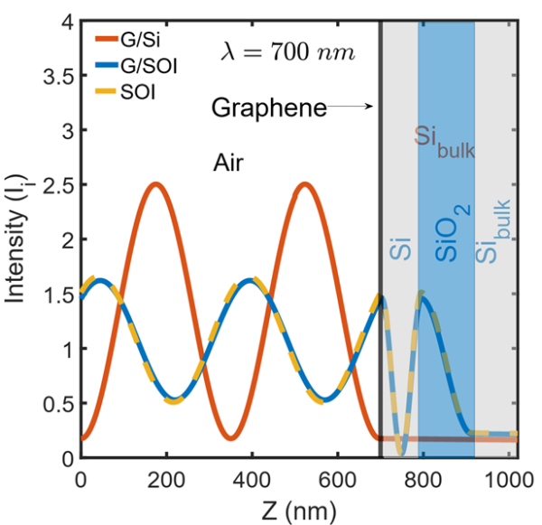
Figure 1 – Time averaged and normalized optical field intensity in the vicinity of the substrate. Bulk Si (red), silicon on insulator (SOI, blue) and silicon on insulator with graphene (G, yellow). Note the larger relative intensity at G/SOI at the air interface and graphene has near to no influence on the intensity at the G/Si junction.
Contact:
Wolfgang Bacsa | wolfgang.bacsa[at]cemes.fr
Publication:
Enhanced light absorption in nanometer-thin graphene-silicon solar cell
E. Rouchy, R. Tan, J. Harmel, M. Respaud, J. Jimenes Jaimes, J.U. Lee, and W. Bacsa
Physical Review B (2026) 114, 305406
DOI: https://doi.org/10.1103/33tj-xn9t
-
Previous Post
Teodor-Aurelian Cucuiet
Related Posts

Women in Computing: Cosmetic Measures and Effective Devices
Thursday, December 3, 2026 Seminar by Isabelle Collet, University of Geneva, Switzerland Open to all
Graphene and ultrathin silicon open a new route to light harvesting
November 17, 2026