Towards a 2D excitonic diode
November 28, 2022
The growth of lateral heterostructures with two different TMD materials is important for the fabrication of new strictly planar devices. Using tip-enhanced optical spectroscopies allowing sub-40 nm spatial resolution, it is shown the nonsymmetric diode-like behavior of a MoSe2/WSe2 lateral heterostructure. Thus, excitons created under the tip in the WeSe2 part can migrate through the junction and recombine in the MoSe2 area. Contrary, excitons created in the MoSe2 part are blocked at the interface due to the energy barrier.
Monolayers of transition metal dichalcogenides (TMD) are extensively studied for their unique optoelectronic properties. TMD heterostructures were initially obtained by stacking two monolayers of two different TMDs, for instance MoSe2 and WSe2. Recently, pure 2D lateral heterostructures (see fig.) have been obtained by chemical vapor deposition by Tuchanin’s group in Iena, then transferred on a substrate encapsulated between h-BN layers, and characterized in the framework of an international collaboration, including researchers from LPCNO and CEMES in Toulouse.
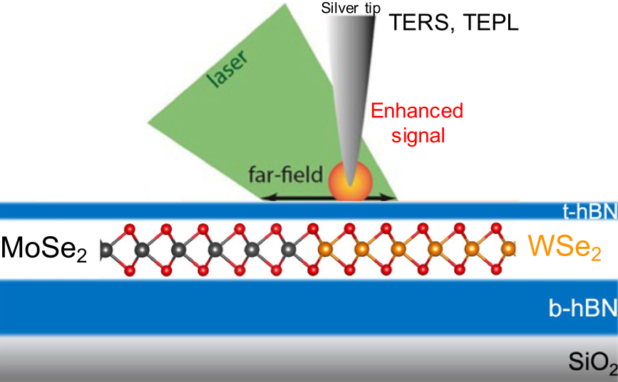
At CEMES, the heterojunction was studied by tip-enhanced Raman spectroscopy (TERS) and tip-enhanced photoluminescence spectroscopy (TEPL), allowing a spatial resolution of 40 nm, about 10 times better than with a standard confocal microscope. The excitation laser is focused on the silver-coated tip, locally enhancing the electric near-field, hence the creation of excitons (an electron-hole pair) in the TMD layer. The PL due to electron-hole pair recombination and the Raman signal are detected and analyzed in each point of the sample. In fact, the sample is raster scanned while recording spectra sequentially with the tip in contact with the surface, and 30 nm above the surface. The near-field contribution is then obtained by taking the difference between both recorded signals.
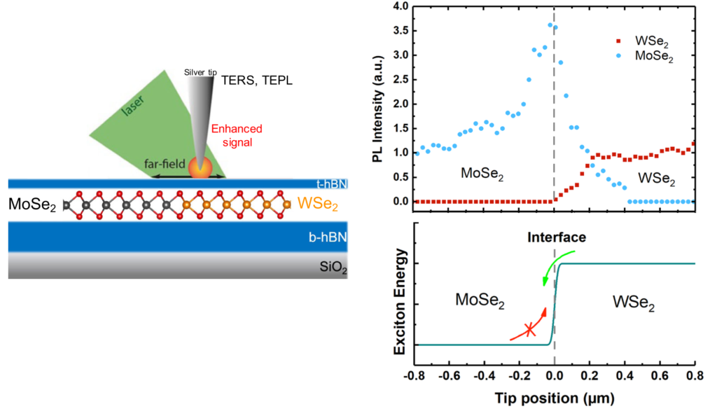
Left: scheme of the tip-enhanced spectroscopy set-up scanning the lateral heterojunction. The improved spatial resolution (40 nm) compared to standard laser spot size (500 nm) is due to the local field enhancement around the tip.
Right: (top) Photoluminescence intensity line scan showing that MoSe2 emission (blue dots) can be detected even when the excitation occurs in the WSe2 region, while WSe2 emission (red dots) is forbidden when the excitation stays in the MoSe2 region. This proves the nonsymmetric excitonic transport due to the energy barrier (bottom) and the lateral heterojunction abruptness.
The TERS mappings delimit the very sharp boundary between both materials with a resolution of about 40 nm, equivalent to the tip diameter at its apex. The TEPL spectra are fitted using a combination of the exciton contributions of MoSe2 and WSe2. The first important result is that a MoSe2 contribution can be detected when the tip is on the WSe2 side, proving that excitons created even far from the interface (up to 400 nm) can diffuse and recombine in the MoSe2 region. In contrary, when the tip is in the MoSe2 region, even close to the interface, no WSe2 contribution is ever detected.
This asymmetric exciton transport behavior, schematically shown in the figure, proves that the lateral heterojunction acts as an excitonic diode, with unidirectional transfer of excitons from WSe2 to MoSe2.
This work was partly funded by projects ANR HiLight (ANR-19-CE24-0020-01) and EUR NanoX 2DLight (ANR-17-EURE-0009). Tip enhanced optical spectroscopies were performed during H. Lamsaadi’s master internship.
Publication:
Exciton spectroscopy and unidirectional transport in MoSe2-WSe2 lateral heterostructures encapsulated in hexagonal boron nitride
D. Beret, I. Paradisanos, H. Lamsaadi, Z. Gan, E. Najafidehagani, A. George, T. Lehnert, J. Biskupek, U. Kaiser, S. Shree, A. Estrada-Real, D. Lagarde, X. Marie, P. renucci, K. Watanabe, T. Taniguchi, S. Weber, V. Paillard, L. Lombez, J.-M. Poumirol, A. Turchanin, and B. Urbaszek.
npj 2D Materials and Applications volume 6, 84 (2022)
https://doi.org/10.1038/s41699-022-00354-0
Contacts:
Jean-Marie Poumirol – jean-marie.poumirol[at]cemes.fr
Vincent Paillard – vincent.paillard[at]cemes.fr
Related Posts

Wolfgang Bacsa
Enseignant chercheur UPS (PR)
Exhibition in the Boule of CEMES
June 7-22 Organised by CEMES with the support of the CNRS and the collaboration of…