The engineering and modeling of charge carriers’ localization in epitaxial QDs
January 23, 2023
Researchers from CEMES, Ioffe Institute and UNICUSANO developed experimentally-verified models for optical emission of epitaxial In(Ga)As and In(Ga)N quantum dots. The models considered In-Ga intermixing, QD reshaping and generation of 3D strain fields. Specific hole wave function at the ground state was determined in In(Ga)As QDs. Novel emission properties were achieved and explained in a multilayer structure with electromechanically coupled In(Ga)N QDs.
Three-dimensional (3D) confinement of charge carriers within epitaxial In(Ga)As and In(Ga)N quantum dots (QDs) allows to considerably improve efficiency of light-emitting diodes and lasers. The engineering of the electron and hole localization in such QDs requires to consider In-Ga intermixing, QD reshaping and generation of 3D strain fields, which are intrinsic processes associated with QDs formation and burying in the bulk of the epitaxial film.
Researchers from CEMES, Ioffe Institute and UNICUSANO developed experimentally-verified models for optical emission of QDs in form of epitaxial In(Ga)As and In(Ga)N 3D islands embedded within GaAs and GaN matrices, respectively. The 3D composition distribution inside the nanometer-size QDs and their geometry were determined by solving the problem of solid mechanics of the stress-strain field inside and around QDs reconstructed from the 2D strain fields measured by dark-field holography in a high-resolution mode.
The parameters of the electron and hole ground states were evaluated in InGaAs QDs by solving the problem of the quantum mechanics within the same finite element model. The results of calculations appeared to be reasonably well consistent with experimentally recorded optical emission spectra. The model revealed a bagel-like shape of the hole wave function at the ground state, being beyond the predictions of simplified models, which should considerably impact the optical and magnetic properties of the QDs.
The 3D character of the strain field created around In(Ga)N islands was exploited to induce their vertical correlation in a multilayer structure. Such an approach allowed for QDs with novel optical properties providing a double wavelength emission in the blue and green spectral ranges. And this despite all layers had the same low In composition, which would have ensured blue emission only. With calculations including electromechanical fields, the modeled optoelectronic properties of a multilayer structure evidenced some optimal In content arrangement in different layers which allowed for a significant reduction of the quantum-confined Stark effect, carrier tunneling through the QDs, an increase of wave functions overlap, and emergence of three distinct peaks in the spectral range, i.e. efficient QDs electromechanical coupling.
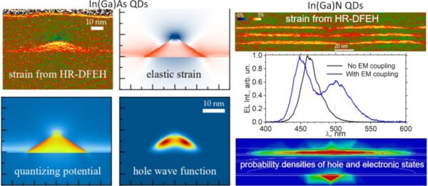
Two dimensional out-of-plane strain maps obtained by dark-field electron holography in high-resolution mode in In(Ga)As (on the left) and In(Ga)N (on the right) QDs used for 3D strain and composition fields reconstruction within finite element and calculations and the modeled optoelectronic properties of such QDs. A bagel-like shape of the hole wave function at the ground state of In(Ga)As QD is revealed. Normalized electroluminescence spectrum from the optimal multilayer structure of In(Ga)N QDs demonstrate double emission arising from electromechanically coupled QDs.
Publications:
Experimentally-Verified Modeling of InGaAs Quantum Dots
Kosarev, V. V. Chaldyshev, and N. Cherkashin
Nanomaterials 12 (12), 1967 (2022)
https://doi.org/10.3390/nano12121967
Electromechanically Coupled III-N Quantum Dots
Barettin, A. V. Sakharov, A. F. Tsatsulnikov, A. E. Nikolaev, and N. Cherkashin
Nanomaterials 13, 241 (2023)
https://doi.org/10.3390/nano13020241
Contact:
Nikolay Cherkashin | nikolay.cherkashin[at]cemes.fr
-
Previous Post
Pablo Simon-Marques
-
Next Post
Christine Viala
Related Posts

Wolfgang Bacsa
Enseignant chercheur UPS (PR)
Exhibition in the Boule of CEMES
June 7-22 Organised by CEMES with the support of the CNRS and the collaboration of…