Infrared localized plasmons without nanolithography
October 1, 2026
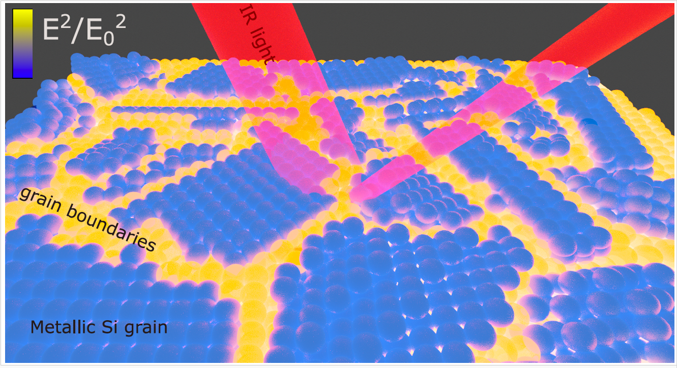
Continuous, hyperdoped nanocrystalline polysilicon films exhibit unique plasmonic behavior that differs from that of conventional metallic layers. By naturally supporting localized surface plasmon resonances, they enable the fabrication of ultra-thin layers—over large areas and without any nanostructuring step—that offer enhanced light-matter interaction.
Localized Plasmon, the collective oscillations of free electrons in metallic or degenerated semiconductor nanostructures, enables the manipulation of light at sub-wavelength scales, down to nanometric dimensions. Major advances in nanofabrication, which paved the way for the development of metasurfaces, have significantly contributed to progress in this field. However, despite rapid advancements, the large-scale deployment of plasmonic metasurfaces remains constrained by challenges related to industrial manufacturing and integration into functional devices.
In a study published in Nano Letters, researchers from CEMES-CNRS, in collaboration with CEA-LETI, demonstrate that an alternative approach is possible: mid-infrared plasmonic resonances can emerge spontaneously in phosphorus-hyperdoped polysilicon layers that lack any artificial nanostructuring. Composed of nanometric grains ranging from 5 to 50 nm in size, these layers exhibit remarkable optical properties that challenge conventional design strategies for plasmonic materials.
By combining advanced techniques in electron microscopy, infrared spectroscopy, and electrodynamic modeling, researchers have demonstrated that these plasmonic responses arise from the natural formation of metal–dielectric contrasts at grain boundaries. These self-organized interfaces thus act as plasmonic nanostructures capable of supporting localized surface resonances.
These results thus position nano-polysilicon as a promising platform for the development of durable, low-cost infrared plasmonic materials, bypassing the complex nanofabrication steps usually required, thereby opening up prospects for new applications, particularly in the thermal management of photovoltaic devices.
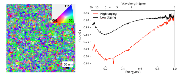
Left : map of the crystal orientations of the phosphorus-doped polysilicon thin film, observed by transmission electron microscopy in plan-view. Right: infrared optical transmission response of the polysilicon layer for two doping levels.
This work was supported by the French National Research Agency (ANR) under the “DIAAPASON” project (ANR-24-CE09-4555), as well as by CNRS-Physique under the Tremplin “PLASMONIX” project.
Contacts:
Caroline Bonafos | caroline.bonafos[at]cemes.fr
Jean-Marie Poumirol | jean-marie.poumirol[at]cemes.fr
Publication:
Emergence of Localized Surface Plasmons in Unpatterned Hyperdoped Polycrystalline Silicon
M. Bahsoun, J. Groenen, G. Agez, S. Joulié, C. Marcelot, R. Cours, S. Kerdiles, S. Opprecht, C. Bonafos, and J. M. Poumirol
Nano Letters (2026): 26 (32)
DOI: https://doi.org/10.1021/acs.nanolett.6c01938
-
Previous Post
Magali Brunet
-
Next Post
PhD defense of Tom Fraysse
Related Posts
Grain boundaries transform silicon into a plasmonic material
October 1, 2026

Magali Brunet
CNRS Researcher